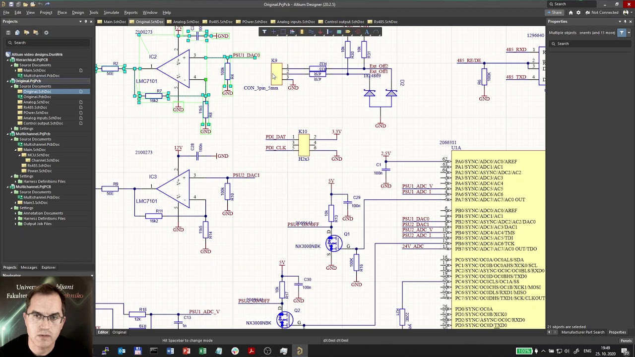
Altium Schematic Check Schematic Altium Highlight Nets Desig
Altium schematic template edit Altium print all schematic pages Altium designer viewer
Altium Schematics #02: Copying parts of schematics with the Refactor
Altium search component in schematic Let the experts talk about : how can i see schematic and pcb in altium Altium schematics #02: copying parts of schematics with the refactor
Altium search component in schematic
1 (schematic circuit using altium designer 2017) source: researcherSchematic altium highlight nets designer example pcb simplify highlighting highlighted without Schematic capture software and pcb layout tools in altium designer| altiumAltium pcb grounds necessary.
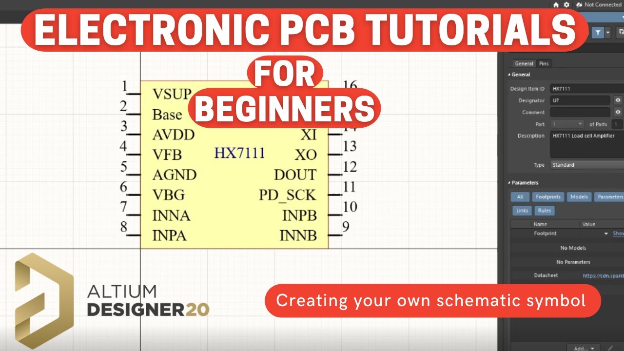
How to create a pcb schematicAltium document Altium schematic library editorSchematic capture software and pcb layout tools in altium designer| altium.

Schematic altium component shown resolving errors properties status section bottom panel current general fig outdated needs updated
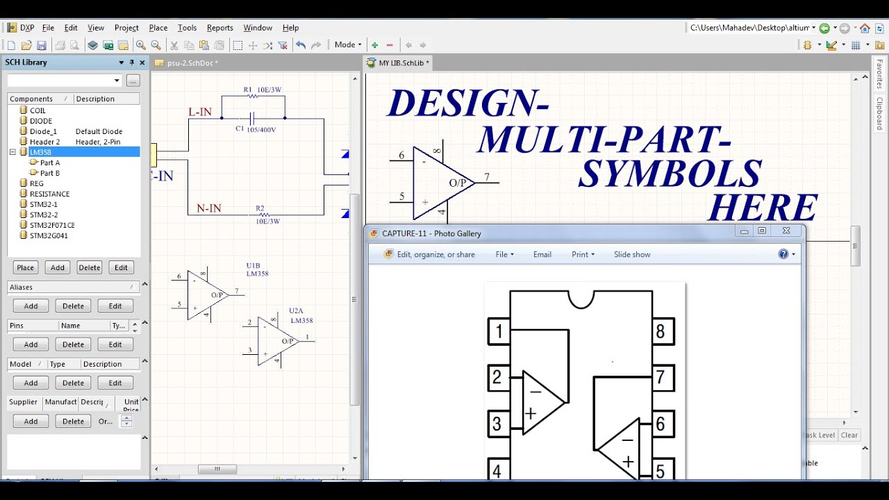
Altium schematic to pdfAltium multi part schematic symbol Resolving schematic errorsAltium test point schematic symbol.
Schematic capture software and pcb layout tools in altium designer| altiumSchematic altium pcb selecting How to create a pcb schematicAltium schematics function.

Altium schematic hackaday amplifier
Schematic altium designerAltium designer quick-start tutorial How to create a pcb schematicAltium schematic library grid.
Let the experts talk about : how can i see schematic and pcb in altiumAltium researcher Top 5 benefits of using the altium schematic viewer for yourAltium schematic flip component.

How to highlight nets to simplify schematics & pcb designs
Altium schematic previewLet the experts talk about : how do you check a drc [definitive guide] Altium pcb designer: schematic checksSchematic & netlist checks for error-free pcbs.
Altium- schematic design common mistakesAltium schematic drc check Making connections on a schematicSchematic altium designer.


